
Bandwidth Breakthrough: New Ultrafast Plasmonic Chip Integrates High-Performance Organic-Electro Optic Material
NLM
- posted on
- No Comment
Tackling growing demands for higher bandwidths, this ultrafast chip that uses light to speed up data transmission in fiber-optic networks and more.
Seattle and Zurich, July 8, 2020 — In an industry first, researchers from ETH-Zurich, University of Washington (UW), and other collaborators have developed an ultrafast plasmonic chip, using light to speed up data transmission. This chip tackles growing demands for higher bandwidths for greater data transmission and computing worldwide. While current technologies are reaching their data transmission speed limits, hybridizing semiconductors and photonics together will unlock our future.
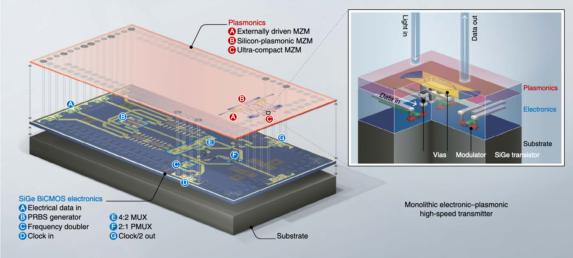
The chip combines several scientific breakthroughs and innovations in device design, materials development, and fabrication processing to achieve its high performance – with practically no loss of signal quality. For the first time, the chip integrates temperature-stable organic electro-optic (OEO) materials with commercially produced BiCMOS electronics. The “HLD” material developed at the University of Washington and used in the chip is readily available from Nonlinear Materials Corporation (NLM).
Today’s optical networks achieve data transmission rates in the region of gigabits (109 bits) per second. As published in Nature Electronics, this new plasmonic chip has achieved rates over 100 gigabits per second without the use of complex modulation schemes. With further refinement, symbol rates beyond 200 gigabits per second should be possible.
Whether it’s streaming technologies or leaps in artificial intelligence, new solutions are needed to take technology devices and infrastructure to the next level. The combination of electronics and optical elements on a silicon platform, along with the reduction in size and increase in speed from the incorporation of plasmonic components and OEO materials, overcomes prior difficulties for dense integration of electronics and photonics.
“This is a key proof point for hybrid electro-optic technologies, demonstrating integration with a commercial process as well as the capability of the latest OEO materials to operate under demanding thermal conditions. Amazing work by the ETH/UW team,” says Dr. Lewis Johnson, Chief Scientific Officer at NLM.
Research groups at UW and ETH-Zurich have collaborated on hybrid electro-optic devices for over six years, leading to dozens of joint publications and conference talks. NLM exclusively licenses, commercially produces, and supplies the UW-developed materials demonstrated in these and other devices, enabling transition of hybrid electro-optic technology to the market.
NLM is a Seattle-based pioneering platform company delivering technology, materials, and full-lifecycle services for organic electro-optic (OEO) materials.
Image: Nature Electronics, doi:10.1038/s41928-020-0417-9