
We’re Celebrating Our 3rd Anniversary!
Gerard Zytnicki
- posted on
- No Comment
NLM Photonics brings photonics to a device in your hands.
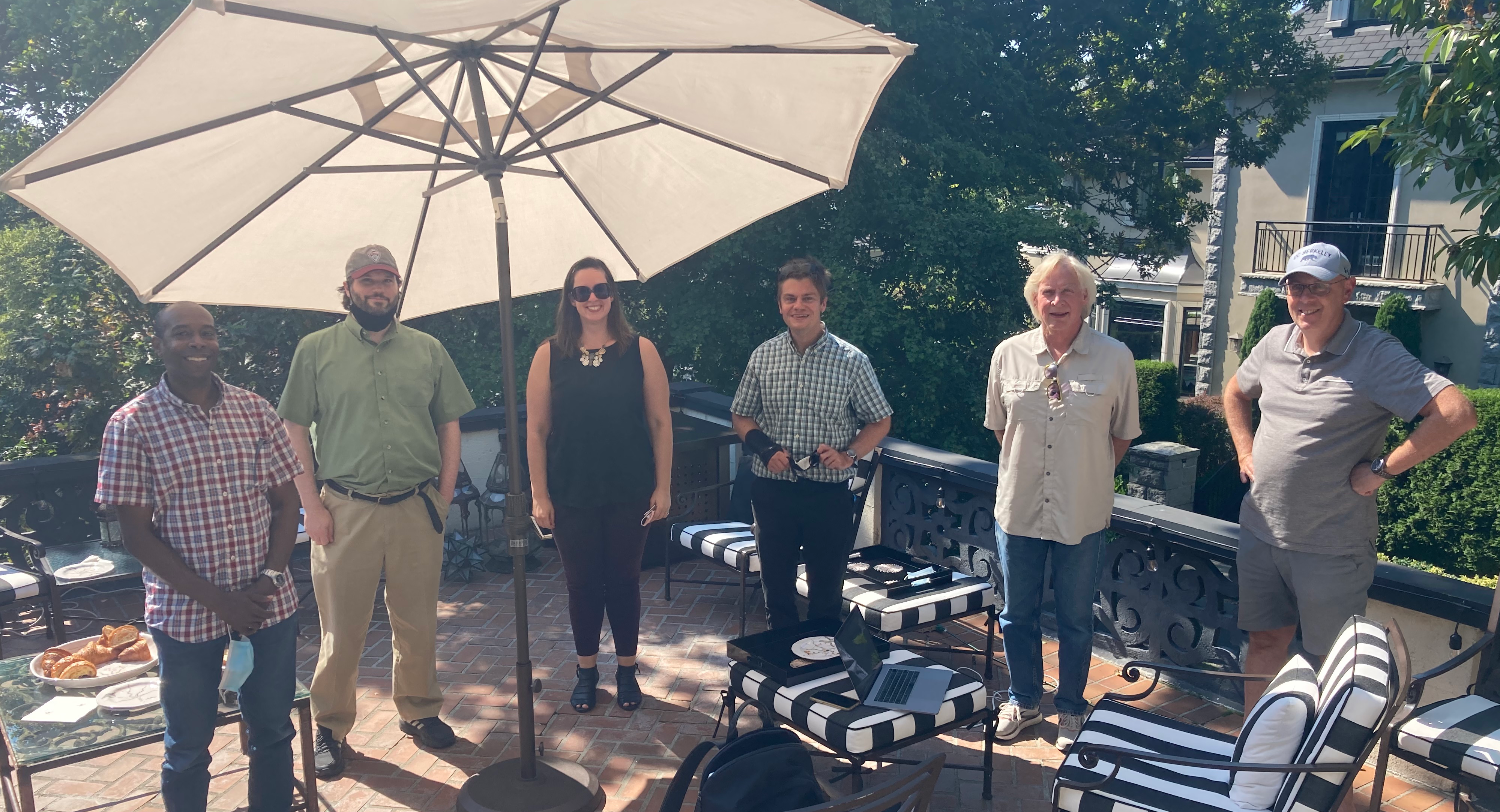
Header photo: Part of the NLM team at an off-site (l-r) — Dr. Delwin L. Elder, Dr. Scott R. Hammond, Dr. Stephanie Benight, Dr. Lewis E. Johnson, Paul H. Nye, and Gerard Zytnicki
Founded in 2018 on a dream of making photonics ubiquitous, at NLM, we’re proud to say we’re achieving this.
From growing our team and funding (including revenue) to expanding our offerings and exciting new R&D, we’re extremely optimistic about the success of our products and industry. August 10th marked our official 3rd anniversary as a company! 🎉
NLM started with three co-founders and two academic contributors/advisors, and now our team’s grown to 10 people, expanding our R&D and other scientific pursuits and leveling up our accounting and marketing efforts. We also maintain an advisory board of nine members, four scientific and five industry leaders, to keep us abreast of industry-specific needs (e.g., wireless and equipment) and funding opportunities.
Our team also continues to grow in their skillset and experiences. Chief Scientific Officer Dr. Lewis E. Johnson recently gave a Keynote speech at SPIE Optics + Photonics, and our Director of Process Development Dr. Scott R. Hammond qualified as an electron beam lithography operator.
We also officially opened NLM Europe, located in Paris, to facilitate the innovation and excitement of European partners and hire local employees.
Opportunities: the global chip shortage and photonics
Here’s what we know: there’s a huge global shortage of semiconductors due to supply chain disruptions and overwhelming demand. The ongoing COVID-19 pandemic amplified this situation, limiting supply due to shutdowns and causing demand for information technology to skyrocket; these effects were compounded by US-specific export control restrictions involving technology trade with China. Everything from our smartphones and computers to our toothbrushes and doorbells requires chips these days. Couple this with high-performance computing desires — quantum, cryptocurrency, AI, and machine learning — and the fact that semiconductors take several months to produce using a very delicate process with hundreds of steps, and you have a big problem.
As companies like Intel, Google, and Apple rush to make their own chips and countries pump billions of dollars into the problem — the US Senate earmarking $52 billion for chips — our industry is heating up dramatically. Not to mention, device innovations and demand further complicate the chip crunch. We need new solutions for providing this connectivity in devices and between them.
This is where photonics comes in.
With higher speed, lower power consumption, smaller size, and potential for dense integration with electronics, photonics overcomes limitations in the current chip market. While creating more chips is essential, faster chips mean fewer chips are necessary for demanding applications like machine learning and telecommunications infrastructure. Plus, climate change demands we be more conscious about our energy and our materials consumption.
Innovation and change are all part of solving the chip problem. However, a key need in photonics is the ability to hybridize with other technology, including traditional CMOS, such that companies don’t have to start from scratch in development. NLM’s materials can integrate into and supercharge existing platforms, meeting this critical requirement.

Growth: Expanding toward the European market
As photonics picks up steam, the European market is particularly interested in innovation beyond conventional semiconductors for their computing and communications needs. Many of the companies we are currently partnering with are based in Europe. They’re extremely enthusiastic about photonics and incorporating our materials into their devices.
In June 2021, we officially opened NLM Europe, located in Paris. We’re currently hiring two scientists based in Europe to work directly with customers. We also started localizing our website content in both French and German to facilitate this connection.
Customer care: Application-specific R&D
Our first commercial materials — JRD1 and HLD — came out of the 20+ years of research conducted at the University of Washington under Profs. Larry R. Dalton and Bruce H. Robinson and their research groups. Peer-reviewed and demonstrated in academic devices, these materials showed that high performance and high stability can be obtained without unacceptable tradeoffs and that organic electro-optic materials (OEO) are commercially viable.
Since then, our R&D has expanded with a focus on stability and electro-optic response. For stability, our materials must integrate seamlessly with other technologies and withstand the intense temperatures — sometimes exceeding 120 °C — very demanding environments require. Dr. Scott R. Hammond tested HLD thoroughly to ensure our customers know precise stability limits.
For electro-optic response, we’ve recently exceeded the long-time goal of 1,000 pm/V record! This exceeds the performance of the best inorganic material, barium titanate. Advanced Materials will publish these achievements, and our R&D team is taking what we learned from this new material for future advancements. Breaking this record is also a long-standing goal for proving the superiority of OEO materials in the marketplace compared to current and other innovative competing technology.
As we continue to work directly with customers, their asks and feedback on our materials relate directly to the applications they are using them for. As Dr. Lewis E. Johnson leads our R&D team to NLM’s next generation of materials, we’re both improving our core performance and exploring application-specific materials for industries with particularly demanding needs, such as quantum computing or aerospace/vehicle applications. Every industry’s unique set of challenges only pushes us to improve with each iteration.

Commercialization: Getting our materials in your devices and in everyday use
Our friends at Polariton Technologies released the world’s first plasmonic-organic hybrid device, powered by NLM’s materials! This ultra-fast, ultra-compact modulator is a game-changer. It’s 3x faster and over 10x smaller than competing products.
And this isn’t the only device in NLM’s future! We are busy working behind the scenes on a few surprises and other proof-of-concept innovations to take OEO to the next realm: scalable commercialization. Decades of research and our R&D proved the power, and now it’s time to get it into products and consumers’ hands.
We’re working to build a bridge between the capabilities enabled by our materials and customer pain points, including making it easier for fabs to integrate our materials into designs and processes.
Photonics is the future: Our vision forward.
With every push, breakthrough, deal, and conversation we have about photonics, it becomes all the clearer that a photonic future will be a reality. We are energized by these past three years, and we are excited for the next three years and beyond!